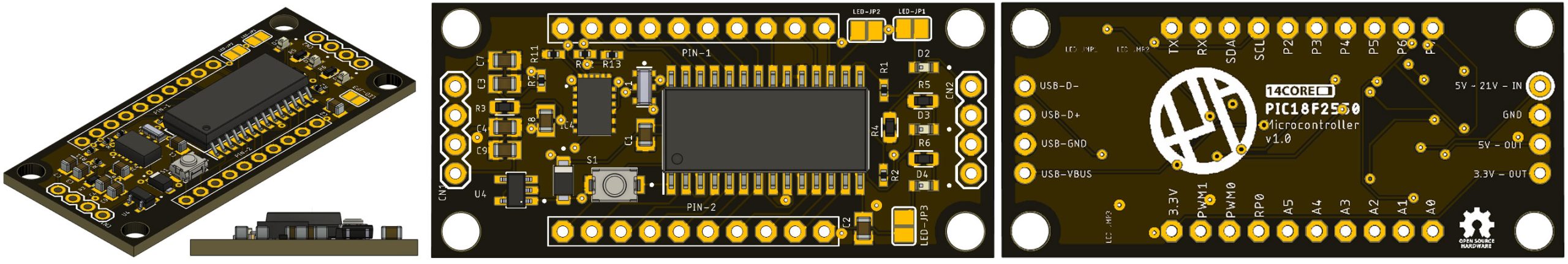
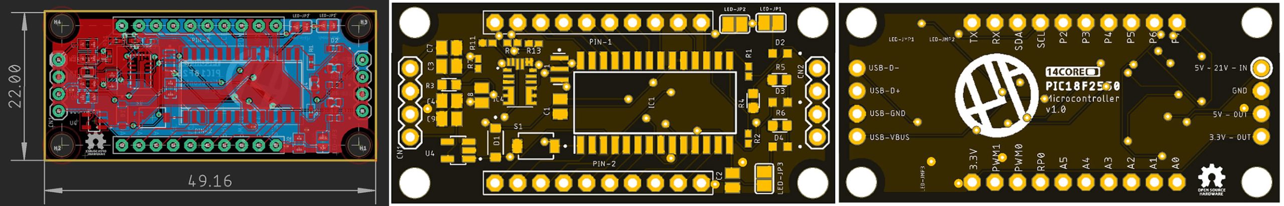
This is the 14CORE PIC18F2550 Minimal Development Board with an input voltage of 4.5v to 21v that can be used in your projects or production purpose, the board has a size of 22X49mm suitable for small and medium size electronic projects. The PIC18F2550 is an 8-bit microcontroller from Microchip It has a maximum CPU speed of 48 MHz and is built on an enhanced flash-based 8-bit RISC architecture. The PIC18F2550 comes in a 28-pin package, making it ideal for applications with space constraints. here are som key features of this microcontroller.
- Flash Program Memory: 32K bytes
- Data Memory (SRAM): 2K bytes
- Operating Voltage: 2.0V to 5.5V
- Maximum Speed: 48 MHz
- Number of I/O Pins: 22
- Analog Inputs: 13
- PWM Outputs: 5
- Timers: 3
This PIC18F2550 microcontroller is equipped with features like USB support, multiple communication interfaces, and a range of on-chip peripherals such as timers, PWM outputs, and analog-to-digital converters (ADCs). It also has a large flash program memory of 32K bytes and a data memory (SRAM) of 2K bytes and is commonly used in a variety of applications, including industrial automation, consumer electronics, and automotive applications. It can be programmed using high-level languages like C or assembly language, and it can be powered by a DC power supply or battery with an input voltage range of 2.0V to 5.5V.
This 14CORE PIC18F2550 microcontroller can be programmed using a variety of programming languages, including C, assembly language, and other high-level languages. Microchip provides a free Integrated Development Environment (IDE) called MPLAB X IDE, which includes a compiler, an assembler, and a debugger for programming PIC microcontrollers. MPLAB X IDE supports C language programming, and it includes a set of libraries and APIs (Application Programming Interfaces) for interacting with the on-chip peripherals and communication interfaces of the PIC18F2550.
To program the PIC18F2550 microcontroller using MPLAB X IDE, you will need to have a programming device like a PICkit programmer or an ICSP (In-Circuit Serial Programming) programmer. These devices connect to the microcontroller through the programming header on the microcontroller board, and they allow you to load the compiled program code into the microcontroller’s flash program memory.
The programming process typically involves the following steps:
- Write your program code in C or assembly language using MPLAB X IDE.
- Compile your program code using the MPLAB X IDE compiler.
- Use a programmer device to connect to the PIC18F2550 microcontroller board through the programming header.
- Load the compiled program code into the microcontroller’s flash program memory using the MPLAB X IDE programmer interface.
Schematics Diagram:
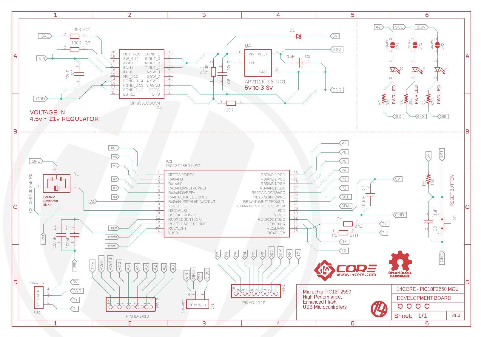
Requirements & Parts List:
| Part | Value | Device | Package |
| C1,C2,C4 | 100nF | Ciramic Capacitor | 0805 |
| C3 | 1uF | Electrolytic Capacitor | 0806 |
| C7, C8 | 22uF | Electrolytic Capacitor | 0807 |
| C9 | 1uF | Electrolytic Capacitor | 0808 |
| D1 | PMEG6020AELRX | Schottky Diode | SODFL3517X110N |
| D2, D3,D4 | KPT-1608ZGC | SMD LED, Red, Green | LED_KPT-1608ZGC |
| IC1 | PIC18F2550-I_SO | Microcontroller | SOIC127P1030X265-28N |
| IC4 | MPM3610GQV-P | Regulator | MPM3610GQVP |
| R1, R2 | 27 Ohms | Resistor | 0402 |
| R3 | 10K | Resistor | 0603 |
| R4,R5,R6 | 330 Ohms | Resistor | 0603 |
| R7, R12 | 100K | Resistor | 0402 |
| R11 | 39K | Resistor | 0403 |
| R13 | 19K | Resistor | 0404 |
| S1 | TL1015AF160QG | Push Button | SW_TL1015AF160QG |
| U4 | AP2112K-3.3TRG1 | Regulator | SOT95P285X140-5N |
| Y1 | CSTCE9M00G55-R0 | Resonator | OSC_CSTCE9M00G55-R0 |
Input Output and Registers Pins :
ANSEL and ANSELH are registers on the PIC18F2550 microcontroller that control the analog input channels.
The ANSEL register (ANalog SELect) controls the analog inputs AN0 through AN7. Each bit in the ANSEL register corresponds to an analog input channel, and setting a bit to 1 enables the analog input function for that channel. When a bit is cleared (set to 0), the corresponding channel is configured as a digital input/output.
The ANSELH register controls the analog inputs AN8 through AN13. It functions in a similar way to ANSEL, with each bit corresponding to an analog input channel. However, since there are only six analog input channels on ANSELH, the remaining two bits are reserved for other functions.
The ANSEL and ANSELH registers allow the PIC18F2550 to selectively enable or disable the analog input function for each channel, which can save power and reduce noise in digital systems where analog inputs are not required. These registers are commonly used in applications where the microcontroller needs to interface with analog sensors or other analog devices.
| ANSEL | |||||||
|---|---|---|---|---|---|---|---|
| 7 | 6 | 5 | 4 | 3 | 2 | 1 | 0 |
| ANS7 | ANS6 | ANS5 | ANS4 | ANS3 | ANS2 | ANS1 | ANS0 |
| ANSELH | |||||||
|---|---|---|---|---|---|---|---|
| 7 | 6 | 5 | 4 | 3 | 2 | 1 | 0 |
| X | X | X | X | ANS11 | ANS10 | ANS9 | ANS8 |
Configuration Example :
|
1 2 3 4 5 6 7 |
ANSEL = 0b10000001; //AN7 and AN0 enabled ANSELH = 0b00000101; //AN8 and AN10 enabled Or we could use hex by: ANSEL = 0x81; //AN7 and AN0 enabled ANSELH = 0x05; //AN8 and AN10 enabled |
TRISA, TRISB, and TRISC are registers on the PIC18F2550 microcontroller that control the direction of the I/O pins in Port A, Port B, and Port C respectively.
The TRISA register (TRIState A) controls the direction of the I/O pins in Port A. Each bit in the TRISA register corresponds to an I/O pin in Port A. When a bit is set to 1, the corresponding pin is configured as an input, and when a bit is cleared (set to 0), the corresponding pin is configured as an output.
Similarly, the TRISB register (TRIState B) controls the direction of the I/O pins in Port B, and the TRISC register (TRIState C) controls the direction of the I/O pins in Port C. Each bit in these registers corresponds to an I/O pin in the respective port.
By setting the bits in these registers, the programmer can configure the microcontroller’s I/O pins as either inputs or outputs. This allows the microcontroller to interface with external devices such as sensors, actuators, and displays.
In summary, the TRISA, TRISB, and TRISC registers are used to set the direction of the I/O pins in Port A, Port B, and Port C, respectively, and are an essential part of configuring the PIC18F2550 for interfacing with external devices.
| TRISA | |||||||
|---|---|---|---|---|---|---|---|
| 7 | 6 | 5 | 4 | 3 | 2 | 1 | 0 |
| X | X | TRISA5 | TRISA4 | TRISA3 | TRISA2 | TRISA1 | TRISA0 |
| TRISB | |||||||
|---|---|---|---|---|---|---|---|
| 7 | 6 | 5 | 4 | 3 | 2 | 1 | 0 |
| TRISB7 | TRISB6 | TRISB5 | TRISB4 | X | X | X | X |
| TRISC | |||||||
|---|---|---|---|---|---|---|---|
| 7 | 6 | 5 | 4 | 3 | 2 | 1 | 0 |
| TRISC7 | TRISC6 | TRISC5 | TRISC4 | TRISC3 | TRISC2 | TRISC1 | TRISC0 |
Configuration Example :
|
1 2 3 4 5 6 7 8 9 10 11 |
TRISA = 0b00110000; //RA5 and RA4 are digital inputs, the rest are outputs TRISB = 0b10010000; //RB7 and RB4 are digital inputs, RB6 and RB5are outputs TRISC = 0b00010001; //RC4 and RC0 are digital inputs, the rest are outputs Keep in mind that any analog pins must be disabled using the ANSEL and ANSELH registers before they can be used as digital I/O. Pin RA3, which is shared with MCLR, is an input only. Therefore, writing to bit 3 of TRISA will have no effect. Reading bit 3 will always return a 1, as RA3 is input only. For example, if you want to use RC0 as a digital output pin you would first have to make sure the ANSEL bit for AN4 was disabled. This is required because it shares a pin with RC0. ANSELbits.ANS4 = 0; //disable AN4 TRISCbits.TRISC0 = 0; //RC0 is a digital output In addition it is a common mistake to set the ANSEL and ANSELH registers incorrect or to forget to set them at all. If you having issues with a digital pin, check ANSEL and ANSELH. bits of ANSEL and ANSELH default to '1' on power on. If you do not set these registers in your code, all the analog pins will be enabled. Therefore, no digital pins that share an analog pin will function correctly. Always set ANSEL and ANSELH. |
PORTA, PORTB, and PORTC are registers on the PIC18F2550 microcontroller that control the state of the I/O pins in Port A, Port B, and Port C, respectively.
The PORTA register controls the state of the I/O pins in Port A. Each bit in the PORTA register corresponds to an I/O pin in Port A. When a bit is set to 1, the corresponding pin is driven high (VDD), and when a bit is cleared (set to 0), the corresponding pin is driven low (VSS).
Similarly, the PORTB register controls the state of the I/O pins in Port B, and the PORTC register controls the state of the I/O pins in Port C. Each bit in these registers corresponds to an I/O pin in the respective port.
By writing to the bits in these registers, the programmer can set the state of the microcontroller’s I/O pins as either high or low. This allows the microcontroller to drive external devices such as LEDs, motors, and relays.
In summary, the PORTA, PORTB, and PORTC registers are used to set the state of the I/O pins in Port A, Port B, and Port C, respectively, and are an essential part of configuring the PIC18F2550 for interfacing with external devices.
| PORTA | |||||||
|---|---|---|---|---|---|---|---|
| 7 | 6 | 5 | 4 | 3 | 2 | 1 | 0 |
| X | X | RA5 | RA4 | RA3 | RA2 | RA1 | RA0 |
| PORTB | |||||||
|---|---|---|---|---|---|---|---|
| 7 | 6 | 5 | 4 | 3 | 2 | 1 | 0 |
| RB7 | RB6 | RB5 | RB4 | X | X | X | X |
| PORTC | |||||||
|---|---|---|---|---|---|---|---|
| 7 | 6 | 5 | 4 | 3 | 2 | 1 | 0 |
| RC7 | RC6 | RC5 | RC4 | RC3 | RC2 | RC1 | RC0 |
|
1 2 3 4 5 6 7 8 9 10 11 12 13 |
ANSELHbits.ANS11 = 0; //Disable AN11 shared with RB5 TRISBbits.TRISB5 = 0; //RB5 is a digital output PORTBbits.RB5 = 1; //Set on the output you can also set RB4 to be a digital input and read it: ANSELHbits.ANS10 = 0; //Disable AN10 shared with RB4 TRISBbits.TRISB4 = 1; //RB4 is a digital input if(PORTBbits.RB4 == 1) //Read RB4 and compare it to 1 PORTBbits.RB5 = 1; //if 1, turn on the output else PORTBbits.RB5 = 0; //if not, turn off the output |
Test Code :
|
1 2 3 4 5 6 7 8 9 10 11 12 13 |
void main(void) { TRISB = 0x00; //Set to use register TRISB PORTB = 0x00; //Set to use PORTB IO while(1) { PORTB = 0xFF; //Set IO enable __delay_ms(50); //Delay 50 milliseconds PORTB = 0x00; //Set IO disable __delay_ms(50); //Delay 50 milliseconds } return; } |
MPLab Test Code :
|
1 2 3 4 5 6 7 8 9 10 11 12 13 14 15 16 17 18 19 20 21 22 23 24 25 |
#include <xc.h> #define _XTAL_FREQ 4000000 #pragma config FOSC=INTRCIO, WDTE=OFF, PWRTE=OFF, MCLRE=ON, CP=OFF, \ CPD=OFF, BOREN=OFF, IESO=OFF, FCMEN=OFF int main() { TRISA = 0xFF; TRISB = 0xFF; TRISC = 0xFF; ANSEL = 0x00; ANSELH = 0x00; TRISBbits.TRISB7 = 0; while(1) { PORTBbits.RB7 = 1; //Set IO enable __delay_ms(500); // Delay 50 milliseconds PORTBbits.RB7 = 0; //Set IO disable __delay_ms(500); // Delay 50 milliseconds } return 0; } |
- Download PCB Milling File | 14CORE PIC18F2550
- Download Gerber Viewer | Windows | Linux
Downloads :
- Download PIC18F2550 Datasheet | PDF
- Download PIC18F2550 Technical | PDF
- Download MPM3610 Step-Down Converter
with Integrated Inductor | PDF - Download AP2112K-3.3 Regulator |PDF